Removing ESD from your cleanroom
Experts estimate that up to one third of printed circuit board (PCB) failures are from electrostatic discharge (ESD). To ensuring reliability in your manufacturing, ESD needs to minimised in any way possible.
Experts estimate that up to one third of printed circuit board (PCB) failures are from electrostatic discharge (ESD). It poses one of the most significant and persistent challenges in cleanroom environments, particularly in industries such as medical electronics, aerospace components, and semiconductor production.
These sectors rely heavily on delicate electrical assemblies that are vulnerable to ESD-induced damages.
This damage can lead to costly warranty returns, time-consuming PCB rework, and even scrapped boards. Not to mention the negative impact to a company’s reputation. Therefore, it’s important to minimise ESD and its impact within cleanrooms.
Understanding ESD
Electrostatic discharge is caused by two surfaces or objects at different levels of electrostatic charge coming into close contact with each other. When one is positively charged, and the other negatively charged, the protons and electrons that carry these charges attempt to balance each other out by rapidly exchanging at the point of contact. The sudden release or discharge of the built-up charge causes an ESD “spike”.
There are two common types of ESD damage: catastrophic and latent
Although ESD is invisible, it is a severe threat in many electronics manufacturing facilities. Static charges of all proportions can cause irreversible damage to delicate electronic components including resistors, capacitors, inductors, diodes, integrated circuits, MOSFETTs, transformers, transistors, integrated circuits, sensors, switches and relays.
Two types of ESD damage
There are two common types of ESD damage: catastrophic and latent. Catastrophic failure causes permanent damage that renders the PCB unusable. Although easier to detect during the inspection, catastrophic damage requires a complete PCB replacement.
Latent ESD damage may not be immediately apparent and often goes undetected during initial inspections. The PCB can be partially degraded and continue to temporarily operate. However, over its lifetime, the component may have compromised or intermittent operational behavior, resulting in an unreliable electronic device.
Although latent damage accounts for the biggest cause of ESD failure, it is also harder to detect. A PCB with latent damage can still be undetected during rigorous testing. This makes failure from latent damage extremely costly to the manufacturer.
Sources of ESD
ESD can occur at any stage of the manufacturing and assembly process, but human touch remains the most common route. The human body and certain clothing can accumulate static electricity levels ranging from 500 to 2,500 volts during a typical workday. Manufacturing areas involving “hands-on” processes, such as receiving, assembly, repair, cleaning, inspection, and packaging, are particularly susceptible to ESD.
Other sources of ESD include ungrounded electrical equipment, such as oscilloscopes used to troubleshoot electronic circuitry. Machinery and other production equipment such as conveyors or carts can also generate friction, and ultimately create ESD as their component materials rub together.
Managing ESD in cleanroom environments
Although it is impossible to prevent all ESD charges completely, there are several ways ESD can be reduced during surface mount technology (SMT) production. Governing bodies such as the International Electrotechnical Commission (IEC) and American National Standards Institute (ANSI) recognise the threat ESD poses to PCBs and include guidelines for ESD control in their standards.
Here are some recommended methods for managing ESD during SMT production:
Environmental control
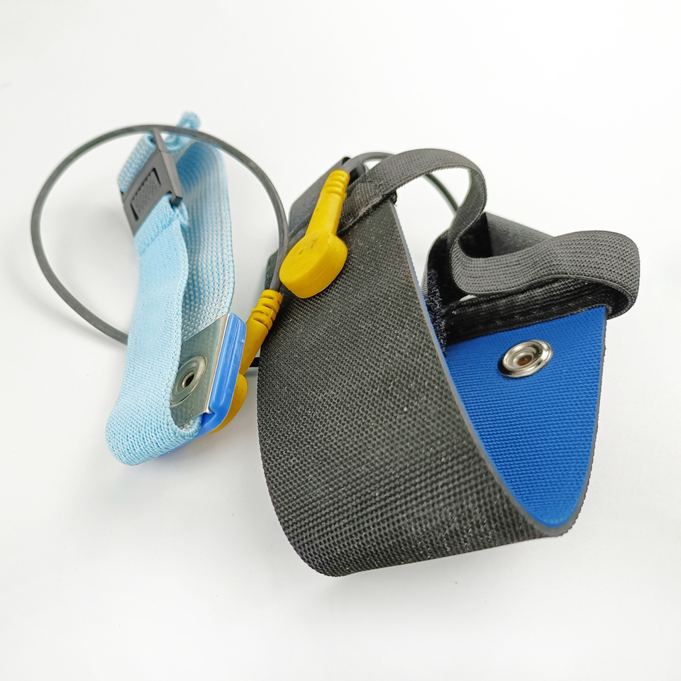
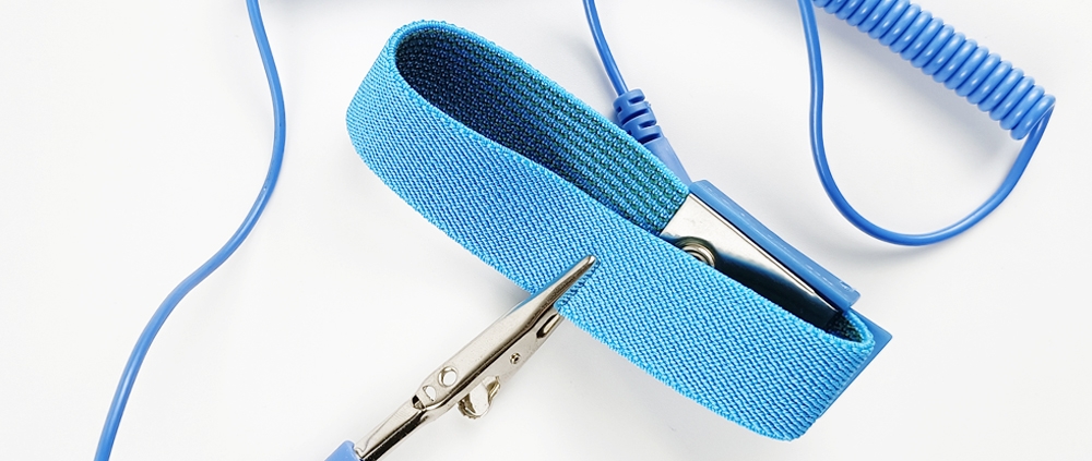
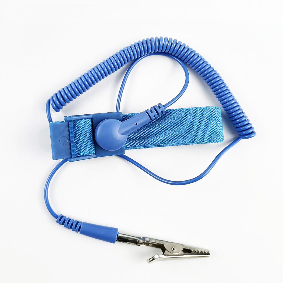
- Use anti-static wrist straps or heel straps connected to a grounded line for workers handling sensitive PCBs. ESD anti-static straps are a simple and effective way of dissipating static from workers. Wrist straps can be connected to a grounded line, keeping the person continuously grounded while they work on sensitive PCBs.
- Install conductive floor mats where technicians walk and stand to discharge static build-up from shoes.
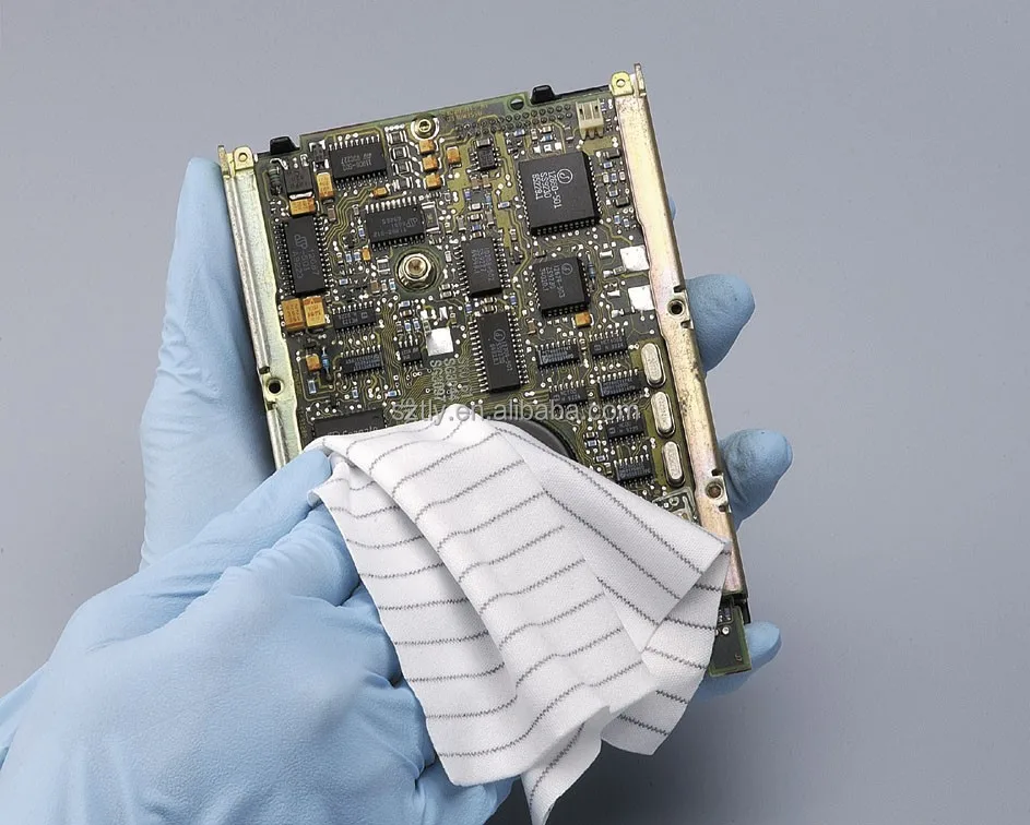
- Ensure workers wear anti-static clothing and shoe coverings.
- Ground all work tables, floor mats, and wrist straps.
- Maintain air humidity between 40-70% and regulate the temperature to 18-22°C (64-70°F) to prevent static build-up. Cooler humid air helps to dissipate static charge.
- Avoid using compressed air for drying PCBs. Fast moving air can cause charge separation, resulting in a build-up of static.
- Remove unnecessary items from the work area that can generate ESD. For example, plastic or polystyrene trays or even notepads and pens can create an ESD charge.
- Ship all assembly parts and PCBs in static-controlled containers and packing materials.