Focusing on the upgrading of the optoelectronics industry, Tailongyu Technology Co., Ltd. showcased its industrial cotton swabs at CIOE Shenzhen Optoelectronics Expo

The 25th China International Optoelectronic Exposition (CIOE Shenzhen), Asia’s largest and most influential optoelectronic information industry event, recently opened at the Shenzhen World Exhibition & Convention Center. As a leading company in the field of industrial precision cleaning, Tailongyu Technology Co., Ltd. participated in the exhibition with its series of industrial cotton swabs specifically designed for the optoelectronic industry. With its precise cleaning solutions adapted to core components such as optical lenses and semiconductor chips, the company’s booth became a “popular booth” during the exhibition, attracting numerous representatives from optical communication, laser technology, and optoelectronic display companies to stop and discuss business.
At this exhibition, Tailongyu Technology Co., Ltd. showcased three core product series:
  • Ultra-fine Fiber Cleanroom Swabs

    Designed for non-destructive cleaning of optical lenses, these swabs are made with ultra-fine fibers (below 0.5μm) and equipped with anti-static handles. They can efficiently remove tiny dust and oil stains on lens surfaces without fiber shedding or secondary contamination. Ideal for precision parts including laser equipment lenses and optical sensors.

  • High-Temperature Sterile Swabs

    Developed for semiconductor packaging and testing, the products can withstand high-temperature sterilization at 121℃, fully complying with strict dust-free and sterile standards for semiconductor workshops. They are widely used for fine cleaning of chip pins and packaging cavities.

  • Miniature Head Precision Swabs

    Customized for Mini/Micro LED display production, the swabs feature a minimum head diameter of 1mm, enabling in-depth cleaning between display pixels and effectively boosting the yield of display panels.

Featuring precise dimensions, high cleanliness and strong adsorption capacity, our industrial swabs fully satisfy the cleaning requirements of precision manufacturing sectors including electronics and semiconductors.
Tailongyu Technology also set up a product demonstration area on site. By simulating scenarios like optical lens cleaning and semiconductor chip packaging, the team vividly presented the products’ outstanding performance in adsorption capacity, wear resistance and zero residue. A purchasing director from a top laser equipment company commented: “Optoelectronic components require extremely high cleanliness. Even a tiny fiber residue will impair equipment performance. Tailongyu Technology’s swabs show low linting and high precision in real tests, which perfectly solves our long-standing cleaning problems in production.”
In response to the industry trend of miniaturization and high integration in optoelectronics, our technical team has reached preliminary cooperation intentions with multiple clients. We will deliver tailor-made cleaning swab solutions matching diverse production processes and application scenarios.
As a long-term exhibitor of CIOE Shenzhen, Tailongyu Technology has been docking with upstream and downstream partners across the optoelectronic industrial chain for three consecutive years. This exhibition further consolidated our leading position in the precision cleaning sector and helped us capture new market demands amid industrial upgrading.
Driven by the booming development of 8K displays, automotive optics, quantum communication and other emerging fields, downstream enterprises have put forward higher requirements for customized and highly adaptable cleaning consumables. Going forward, Tailongyu Technology will keep focusing on the core cleaning challenges of the optoelectronic industry, scale up R&D investment and optimize product performance. We will continue to deliver more efficient and accurate cleaning solutions for industry players, and contribute to the high-quality development of the global optoelectronics industry.

Fiber optic cleaning swabs see a sharp surge in demand,Global Optical Modules 2026: Driven by AI Computing, Accelerated by Domestic Leaders

In 2026, the global optical module industry has officially entered a scale explosion period driven by AI computing power. The industry features a core landscape of high market growth, full release of 800G products, large-scale commercial landing of 1.6T solutions, simultaneous development of Silicon Photonics, LPO and CPO technologies, as well as rising dominance of domestic supply chains, gradually becoming the core engine leading the development of the global optical communication industry.With the rapid development of related industries, the market demand for fiber optic cleaning swabs has continued to surge.

1. Market Size: AI Demand Surging, 800G & 1.6T Become Core Growth Drivers

Driven by the dual growth momentum of full-scale shipment of 800G optical modules and large-scale commercial application of 1.6T products, the global optical module market will achieve leapfrog development throughout 2026.
• Data Center Core Demand: Overseas large-scale computing center construction continues to accelerate. Supported by NVIDIA GB300 series chips, the industry gradually popularizes the matching solution of 1.6T switch end plus 800G network card end, which contributes more than 70% market increment.
• Telecom Network Steady Recovery: The continuous advancement of 5G-A construction and backbone network upgrading steadily boosts market demand for 400G and 800G coherent optical modules.
• Automotive Optical Communication Emerging Track: The automotive optical communication market officially enters the commercialization era, with an annual growth rate exceeding 45%. 10G optical modules are widely applied in smart cockpit and autonomous driving transmission scenarios.
• Domestic Manufacturers Leading the Global Market: Chinese optical module enterprises occupy more than 70% of the global market share. The export volume maintains a steady year-on-year increase, and high-end high-speed product orders of leading enterprises have been scheduled till 2028.
However, within the optical module manufacturing sector, these modules frequently require cleaning. Our company produces specialized optical swabs designed to help enterprises resolve this common challenge. These swabs are suitable for use in the optical industry—specifically for cleaning fiber optic connectors, optical modules, camera lenses, microscopes, and laser optics—as well as in the electronics and semiconductor sectors for cleaning PCBs, hard drive read/write heads, and SMT production lines. Additionally, they serve as precision cleaning tools and are ideal for laboratory sampling applications.

2. Technological Evolution: Speed Upgrade Accelerates, Low-Power Consumption Solutions Mature

In 2026, the core direction of industrial technology iteration focuses on speed improvement, power consumption reduction and cost optimization. Multiple low-power technical routes achieve mature application and differentiated scenario matching.
• High-Speed Product Iteration Accelerates: 800G optical modules become the mainstream standard configuration in AI data centers; 1.6T optical modules realize stable mass delivery. Meanwhile, ultra-high-speed optical module products such as 12.8T are continuously launched, laying a foundation for future ultra-large-scale computing cluster interconnection.
• Multi-dimensional Cost Reduction Takes Effect: The overall industrial capacity utilization rate stays above 90%. The localization rate of high-end core optical chips keeps rising to 50%, effectively cutting down industrial costs and reducing dependence on imported core components.
• Intelligent Operation & Maintenance Popularized: Optical modules are equipped with built-in intelligent health monitoring chips, which support real-time data monitoring, remote fault early warning and automatic performance calibration, effectively reducing overall network operation and maintenance costs by 30%.

3. Industrial Chain Pattern & Industry Future Outlook

The optical module industry steps into the dual competition stage of technology strength and production scale, and market resources further gather towards leading enterprises with core advantages.
• Deep Vertical Industrial Chain Integration: Leading manufacturers continue to increase investment in independent research and development of core components, realize mass production of high-performance silicon optical chips, and steadily raise the self-supply ratio of core devices. Enterprises actively deploy overseas production bases to optimize global supply chain layout.
• Close Industrial Ecological Cooperation: A complete cooperative ecosystem jointly built by AI chip manufacturers, switch suppliers and optical module suppliers has taken shape. Domestic enterprises continuously enhance their discourse power in the formulation of global high-speed optical module industry standards.

Industry Future Prospect

• In the short term, the large-scale shipment of 800G and 1.6T high-speed optical modules will continue to support the sustained high prosperity of the industry.
• In the medium term, higher-rate products such as 3.2T and 6.4T will gradually complete technical maturity and market verification, and CPO technology will become the mainstream configuration for large-scale AI computing clusters.
• In the long run, with the full realization of domestic independent controllable industrial chain, the optical module industry will further expand emerging application markets such as vehicle-mounted communication and satellite communication.

Practical Strategic Suggestion

• For industry enterprises, it is essential to increase R&D investment in Silicon Photonics, LPO and CPO core technologies, and reasonably expand production capacity of high-speed optical modules.
• For market investors, priority can be given to high-speed optical module track, domestic alternative optical chip field and CPO emerging technology sector.

Applications and value of dust-free cotton swabs in the optoelectronic field

        With the rapid iteration of 8K ultra-high-definition display, AI machine vision and gigabit optical network technologies, the manufacturing of optoelectronic displays and optical instruments has entered an era of precision competition at the micron and even nanometer levels. In this high-end and sophisticated field, tiny particle contamination or organic residues have become a key bottleneck restricting product yield and performance. As a core consumable for micro-nano cleaning processes, dust-free swabs are gaining increasingly prominent application value in scenarios such as lens sensors, display panels and optical fiber communication.

Precision Optical Cleaning: Dual Guarantee of Zero Residue and Anti-Static Performance

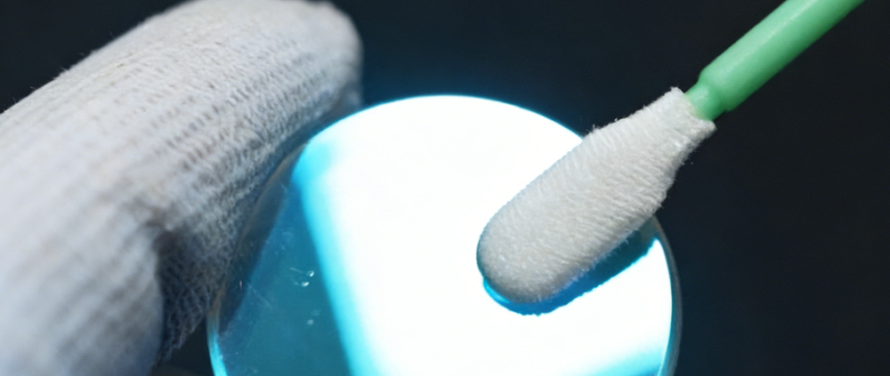
        In the assembly and maintenance of high-end camera lenses, microscope objectives and CCD/CMOS image sensors, surface cleanliness directly determines the imaging quality of optical systems. Traditional wiping materials are prone to fiber shedding and electrostatic adsorption, which may cause permanent dark spots on sensors or induce thermal lens effect on laser lenses due to oil residues under high-energy irradiation.
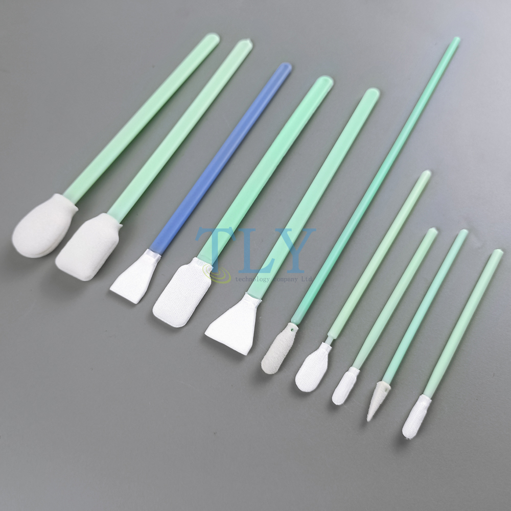
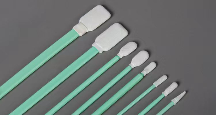
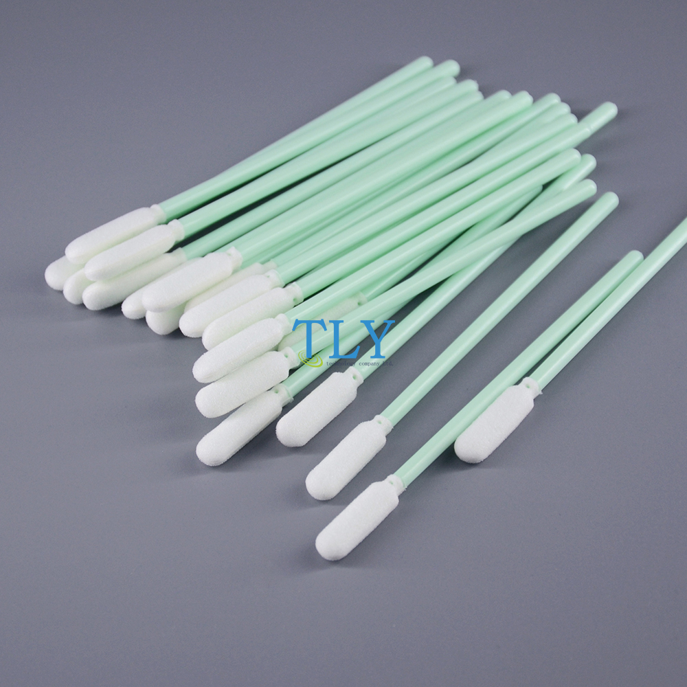
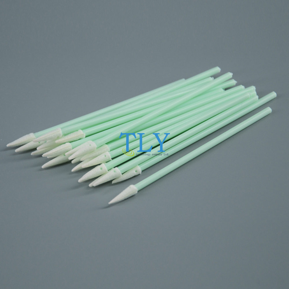
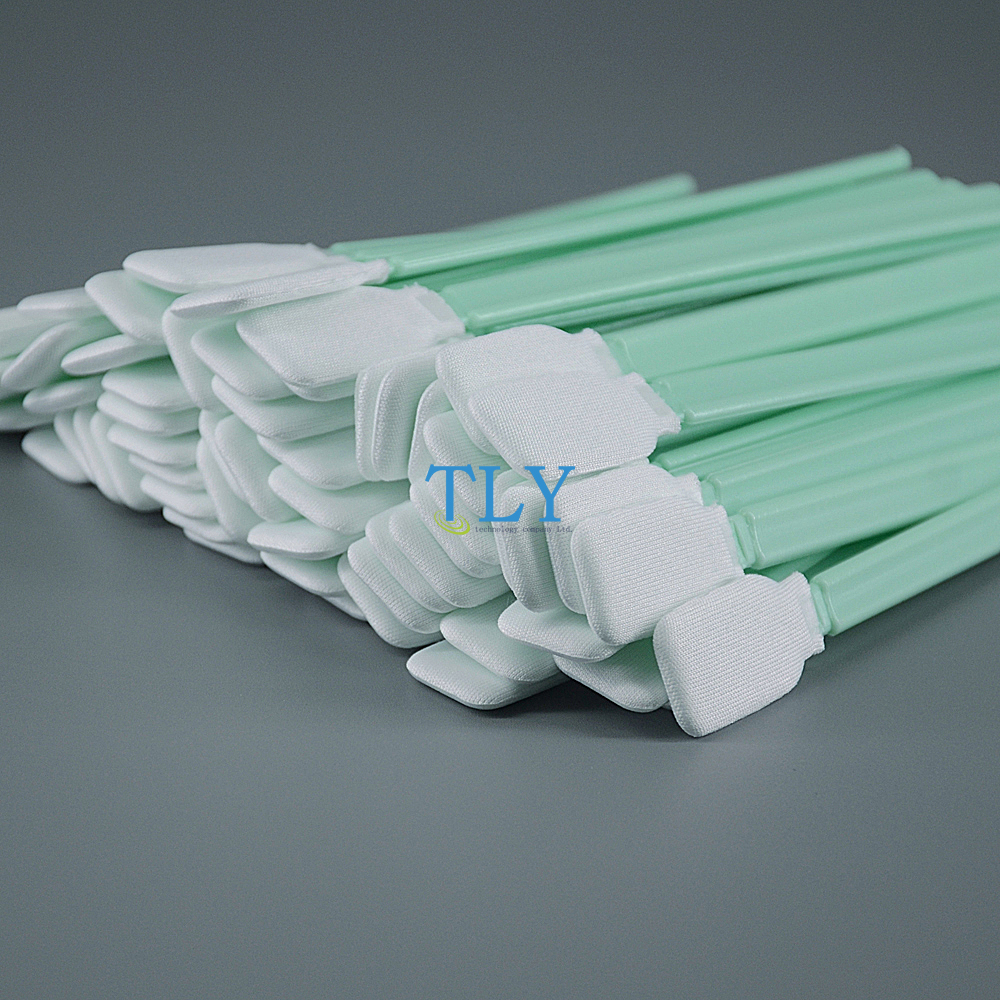
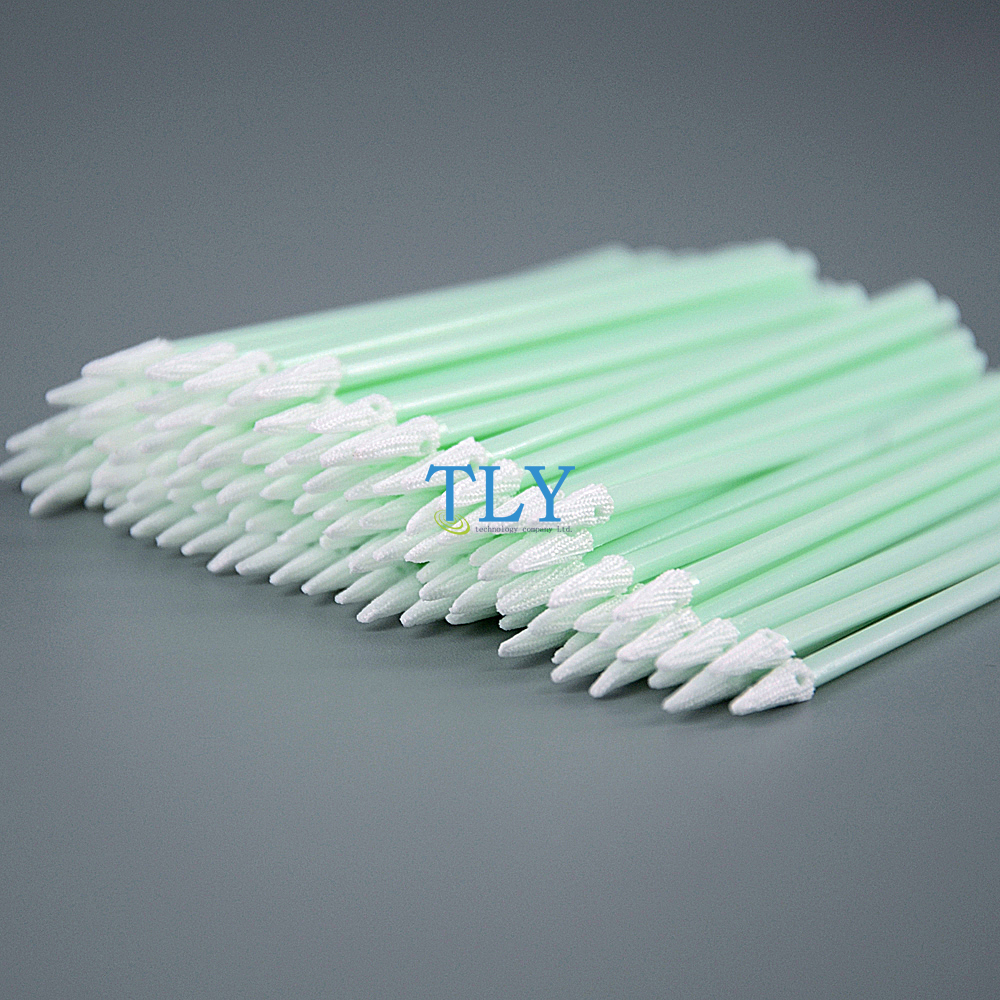
        Professional dust-free swabs applied in this scenario adopt ultra-fine polyester fiber or wood-pulp composite tips, and apply a unique heat-sealed edge process to eliminate the risk of lint shedding from the source. Their core technical features include extremely low particle count and built-in high-efficiency anti-static agents. This design can not only effectively absorb micron-level dust, but also prevent secondary contamination, ensuring absolute surface purity of highly sensitive sensors and laser optical components, and serving as a reliable “first line of defense” for precision optical systems.

Display Panel Manufacturing: Chemical Compatibility and Precise Operation

        In the production process of LCD and OLED panels, the cleanliness of glass substrate edges, polarizers and touch modules directly affects the final visual display effect. Any tiny residue may develop into irreparable bright spots or dead pixels after packaging, resulting in scrapping of high-value panels. Especially in the field of flexible OLED, the high sensitivity of materials imposes stricter requirements on cleaning tools.
        High-grade dust-free swabs exhibit excellent solvent compatibility in this process. Whether using isopropyl alcohol (IPA) or special cleaning solutions, high-quality swab tips maintain structural stability without swelling or degumming. Their elaborately designed handles (made of polypropylene or bamboo) enable precise force control, which can effectively remove flux residues and oil stains while avoiding scratches on flexible materials caused by excessive force. Such precise operability significantly reduces the occurrence rate of bright spots and dead pixels during production, acting as a critical detail for improving panel yield.

Optical Fiber Communication Maintenance: Standardized Tool for End-face Treatment

        Against the backdrop of explosive growth in bandwidth demand at data centers, the cleaning quality of optical fiber connector end-faces (such as FC/SC/LC interfaces) is crucial to the stability of optical signal transmission. Tiny contamination on the end-face will lead to a sharp increase in insertion loss and excessive return loss, further causing network outages.
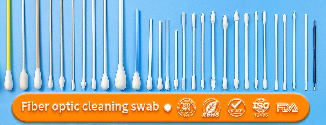
        For optical fiber communication scenarios, the low ion precipitation property of high-purity dust-free swabs is essential. These products undergo strict cleanroom cleaning and vacuum packaging to ensure no silicone oil or plasticizer residues. When used with precision cleaners, they can quickly dissolve oil stains on end-faces with rapid volatilization and no water marks left. Their standardized operating procedures and reliable cleaning effect make them an indispensable tool for ensuring low-loss optical transmission and realizing standardized operation and maintenance.

Future Trends of Micro-Nano Cleaning Processes

        From material selection to production processes, modern dust-free swabs are no longer simple wiping tools, but high-tech consumables complying with the latest international standards such as ISO 14644-5:2025. Their outstanding performance in low dust generation, high purity and precise operation provides a solid microscopic foundation for the optoelectronic industry to address the challenges of high-precision manufacturing.
        Faced with increasingly stringent industry standards, the standardized use of high-grade dust-free swabs is not only a necessary measure for enterprises to enhance process capability, but also a core driving force for ensuring the performance of optical systems and promoting high-quality development of the optoelectronic industry. On the path pursuing extreme light and shadow as well as high-speed transmission, rigorous control over microscopic details will determine the future competition pattern.

C-CUBE builds its first large modular vaccine facility in Europe

C-CUBE has installed modules directly outdoors, encompassing both the facility and the cleanroom area of its first large modular vaccine facility build in Europe.

The Singapore-based company specialises in modular facilities for the life sciences and its smart Cleanroom Modules are self-sufficient and suitable for installation into any existing infrastructure.

The cleanroom modules can also stand alone as a facility and the facility will still be Current Good Manufacturing Practices (cGMP) compliant.

Modular vaccine facilities are designed for flexibility, enabling quicker construction and operation compared to traditional facilities.

C-Cube’s innovation could enhance vaccine manufacturing capacity in Europe and support rapid responses to pandemics and other health crises.

“This success is setting the stage for rapid growth and development in the coming years. I would like to extend my heartfelt gratitude to all the companies and individuals who have supported us throughout this journey, helping to turn our vision into a remarkable reality,” Co-Founder & CEO  of C-CUBE, Christophe Mermaz, posted on LinkedIn.

Cleanroom build expert CAI Engineering completes ISO Class 6 operating rooms

CAI Engineering has completed the design and installation of the Ultra Clean Ventilation (UCV) system for four operating rooms at Rajavithi Hospital in Bangkok, Thailand.

The operating rooms have been certified at ISO Class 6 cleanliness in accordance with ISO 14644-1 standards.

The Thailand-based cleanroom specialist completed this healthcare project in two months.

Further, in terms of sustainability, the new UCV system maintains an environment at 20°C with 50% relative humidity and requires 7.56 kW of cooling, which is “dramatically lower than conventional systems, yet it still ensures maximum performance in creating a sterile surgical space,” according to CAI Engineering.

CAI Engineering is a global engineering firm that specialises in providing commissioning, qualification, validation, and consulting services primarily for life sciences industries, including pharmaceuticals, biotechnology, medical devices, and healthcare.

The main focus of CAI Engineering is on ensuring that facilities, systems, and equipment meet regulatory requirements, operate efficiently, and perform reliably to maintain product quality and safety.

Modular cleanroom expert Pharmadule expands in France

Pharmadule, a Sweden-based expert in design and construction of modular pharmaceutical manufacturing facilities, has opened a new sales office in France.

Pharmadule Morimatsu Business Development Director, Frederic Faiz, will manage the sales office in France.

“This strategic move allows us to better serve our clients in France and the French-speaking markets in Europe, with our innovative modular facilities and customised process equipment,” the VP of Pharmadule, Jens Lindgren, commented in a LinkedIn Post.

With this new office, Pharmadule also intends to collaborate with local partners.

Pharmadule is a Morimatsu Group company, which is a multinational company that manufactures and supplies process equipment and modular facilities to a variety of industries.

The group includes Morimatsu International Holdings, as well as Pharmadule.

AM Technical Solutions expands in Malaysia to support semiconductor cleanroom builds

US-based AM Technical Solutions is investing significantly in semiconductor markets throughout Asia.

The company has recently announced expansion plans in India, and is now expanding its presence in Malaysia.

The expanded presence in Malaysia will be in the form of a new office in Penang, Malaysia. “[This] will enable us to support our semiconductor customers by providing the specific resources they need to support capital projects,” the company stated.

“Additionally, we are helping the local contractors on the ground in Malaysia understand our customers’ needs to ensure project requirements are satisfied on tight timelines,” the company added.

The Malaysian market

Malaysia’s semiconductor boom is centred in the northern state of Penang.

With semiconductor projects being AM’s core business they stand to be able to help both new facilities and expansion projects. For example,

“For example, we are currently supporting a backend facility in Kulim, where semiconductor activity is bustling,” the company stated.

“We are primarily focusing on providing commissioning, construction management, and Quality Assurance/Quality Control (QAQC) to validate that projects are completed according to industry requirements through a first-time-right approach,” the statement explained.

“By establishing a new office in Malaysia, we can maintain visibility into each project and provide prompt solutions to resolve any issues.”

“When asked by our customers to support semiconductor projects in Malaysia, we gladly agreed to help,” said Sandeep Davé, Chief Business Officer. “Our proven experience will enable us to build a local pool of talent to support our customers in Malaysia and provide a cost-efficient solution for each project.”

PBSC redesigns cleanroom air shower for functionality

UK-based PBSC has redesigned its air shower.

The cleanroom and containment expert’s Air Shower is a specialised enclosure designed for cleanrooms and controlled environments. Reducing the risk of particulate contamination from personnel before entering or exiting critical areas.

The product has been redesigned to enhance not only the aesthetics but also the functionality.

The high-performance fans are now strategically fitted to each side wall, ensuring optimal airflow through each plenum for more effective decontamination for personnel.

Jamie Davis, PBSC company owner, explained: “Widely used in industries such as pharmaceuticals, biotechnology, semiconductor manufacturing, and food processing, PBSC’s Air Shower is essential for maintaining high standards of cleanliness and contamination control.”

Davis added: “We are proud to have contributed to a number of prestigious projects with our personnel decontamination shower, and with our latest enhancements, we ensure an even smoother experience for facilities staff.”

Key features of PBSC’s Air Shower:

  • High-performance air jets: Powerful air jets effectively remove dust, lint, and other contaminants from personnel – Air velocity of 30 to 34 m/s through 38mm diameter nozzles.
  • Durable construction: Made from robust materials like 304 or 316 stainless steel or powder-coated steel, the air shower is built to withstand rigorous use and ensure long-term reliability with no side service access required.
  • Compact design: The final assembly is designed to fit through a standard single doorway eliminating the need for cranes or special access during installation.
  • Advanced control systems: The shower includes user-friendly controls for efficient operation and can be customized to meet specific requirements.
  • High flow upgrade option with 3800m³/hr airflow capacity available.

The building has to “rest in itself”: CRC tops out on wafer fab for Vishay

Vishay has topped out on its new hi-tech fab in Itzehoe, Germany.

The expert in discrete semiconductors and passive electronic components has invested around $400m in the new 12′ wafer fab.

The expansion was needed as the US-based group’s existing factory reached its limits.

For the build’s Engineering, Procurement, and Construction Management (EPCM), Vishay has contracted Germany-based Clean Room Consulting (CRC).

CRC provides hi-tech facility services such as cleanroom planning and laboratory planning.

Germany-based CRC is also acting as EPCM partner for other projects, such as the Jenoptik semiconductor fab in Dresden, which started interior work in February 2024.

Itzehoe

The new facility is planned to manufacture products for the automotive industry, hosting around 150 employees.

According to Timo Porta, Managing Director at CRC: “The building has to “rest in itself” in order to ensure the extremely high production quality in the nanometer range. A lot of concrete – a total of around 80,000 tons of concrete will be used – and the waffle elements installed a few months ago ensure that even the smallest vibrations can be avoided.”

Originally announced to cost around €300-350m according to EE Times Europe, the new facility is now estimated to cost €374m.